Driver IC ST7789V
General Description
The ST7789V is a single-chip controller/driver for 262K-color, graphic type TFT-LCD. It consists of 720 source line and 320 gate line driving circuits. This chip is capable of connecting directly to an external microprocessor, and accepts, 8-bits/9-bits/16-bits/18-bits parallel interface. Display data can be stored in the on-chip display data RAM of 240x320x18 bits. It can perform display data RAM read/write operation with no external operation clock to minimize power consumption. In addition, because of the integrated power supply circuit necessary to drive liquid crystal; it is possible to make a display system with the fewest components.
Features
1. Single chip TFT-LCD Controller/Driver with On-chip Frame Memory (FM)
2. Display Resolution: 240*RGB (H) *320(V)
3. Frame Memory Size: 240 x 320 x 18-bit = 1,382,400 bits
4. LCD Driver Output Circuits
a. Source Outputs: 240 RGB Channels
b. Gate Outputs: 320 Channels
c. Common Electrode Output
5. Display Colors (Color Mode)
a. Full Color: 262K, RGB=(666) max., Idle Mode Off
b. Color Reduce: 8-color, RGB=(111), Idle Mode On
6. Programmable Pixel Color Format (Color Depth) for Various Display Data input Format
a. 12-bit/pixel: RGB=(444)
b. 16-bit/pixel: RGB=(565)
c. 18-bit/pixel: RGB=(666)
7. MCU Interface
a. Parallel 8080-series MCU Interface (8-bit, 9-bit, 16-bit & 18-bit)
b. 6/16/18 RGB Interface(VSYNC, HSYNC, DOTCLK, ENABLE, DB[17:0])
c. Serial Peripheral Interface(SPI Interface)
d. VSYNC Interface
8. Display Features
a. Programmable Partial Display Duty
b. CABC for saving current consumption
c. Color enhancement
9. On Chip Build-In Circuits
a. DC/DC Converter
b. Adjustable VCOM Generation
c. Non-Volatile (NV) Memory to Store Initial Register Setting and Factory Default Value (Module ID, Module Version, etc)
d. Timing Controller
e. 4 preset Gamma curve with separated RGB Gamma setting
10. Build-In NV Memory for LCD Initial Register Setting
a. 8-bits for ID1 setting
b. 8-bits for ID2 setting
c. 8-bits for ID3 setting
d. 46-bits for VCOM Offset adjustment
11. Driving Algorithm
a. Dot Inversion
b. Column inversion
5. Wide supply Voltage Range
a. I/O Voltage (VDDI to DGND): 1.65V ~ 3.3V (VDDI VDD ≦ )
b. Analog Voltage (VDD to AGND): 2.4V ~ 3.3V
6. On-Chip Power System
a. Source Voltage (VAP (GVDD) to VAN (GVCL)): +6.4~-4.6V
b. VCOM level: GND
c. Gate driver HIGH level (VGH to AGND): +12.2V ~ +14.97V
d. Gate driver LOW level (VGL to AGND): -12.5V ~ -7.16V
e. Adjustable voltage range for feed through compensation: 0.1V~1.675V
7. Optimized layout for COG Assembly
8. Operate temperature range: −30℃ to +85℃
9. Lower Power Consumption
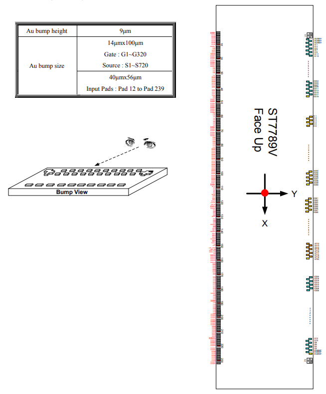
Pad Arrangement
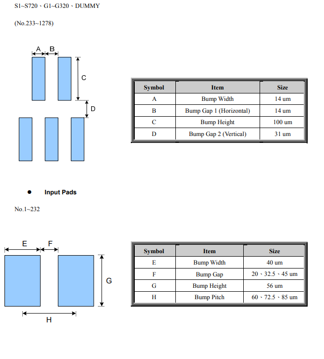
Output Bump Dimension

Output Pads

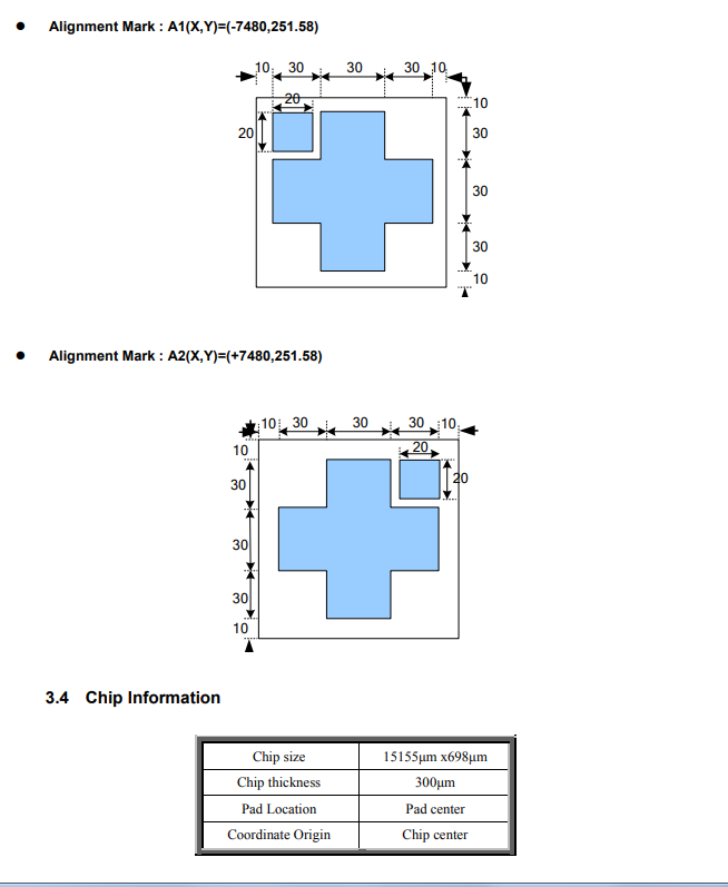
Alignment Mark Dimension


 Microsoft Teams
 WhatsApp
 Email
Email Inquiry
 WeChat
 TOP
TOP